Technology
SEM Technology Overview – Scanning Electron Microscopy
The information below is provided only as a general overview of Scanning Electron Microscopes and the imaging and analysis they can provide. The interested reader is encouraged to explore some of the much more thorough reviews found in books and around the web. Here are a few that we recommend:
- MyScope Training by AMMRF (Australian Microscopy & MicroAnalysis Research Facility
- MyScope Outreach – a step-by-step narrated explanation and simulator
- Practical Electron Microscopy
See more references at our LINKS page
Interaction between electron and solid
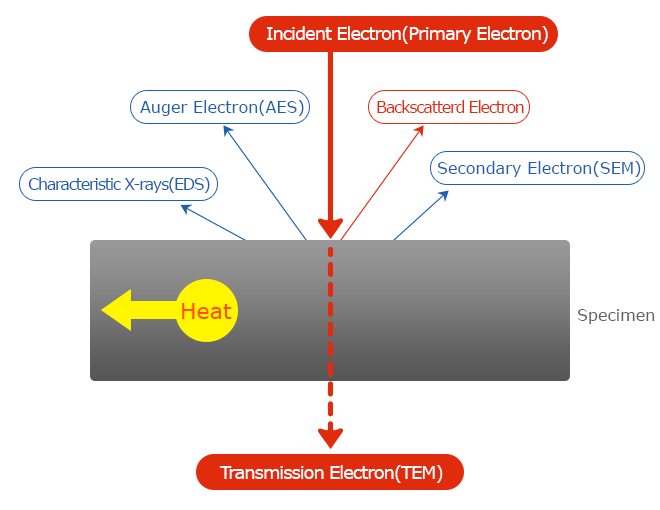
SEM Overview
Optical Microscope
Low resolving power, Low depth of focus
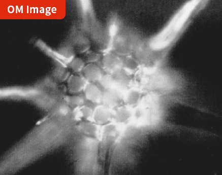
Scanning Electron Microscope
High resolving power, High depth of focus

Overview of Scanning Electron Microscope Components
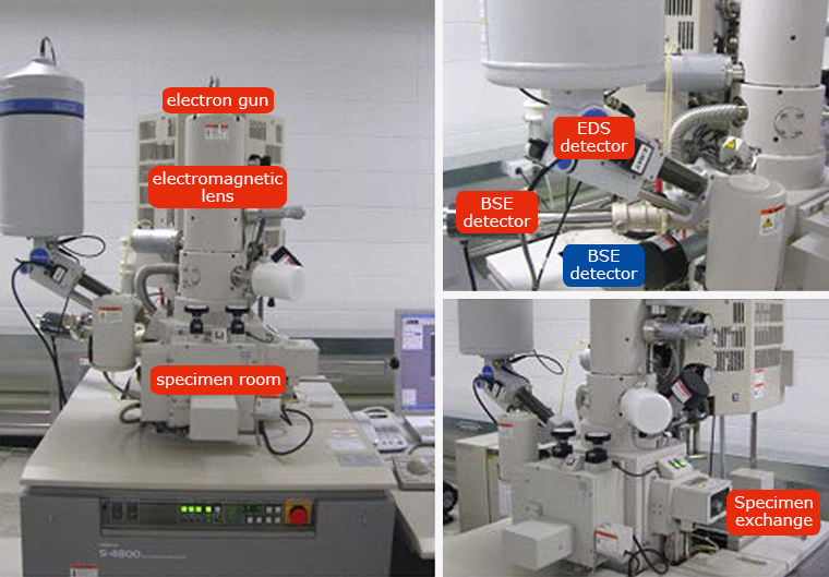
SE (Secondary Electron)
Electron emitted backwards elastically when incident electron beam collided with the specimen
BSE (Backscattered Electron)
Electrons having energy less than 50eV generated in the specimen by inelastic collision of electronic beam and the specimen when incident electron beam collided with the specimen
SEM Overview
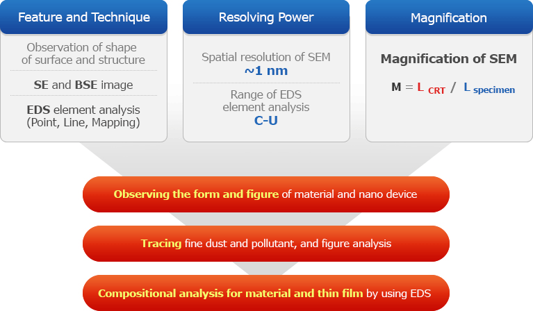
Schematic of Scanning Electron Microscope internal components
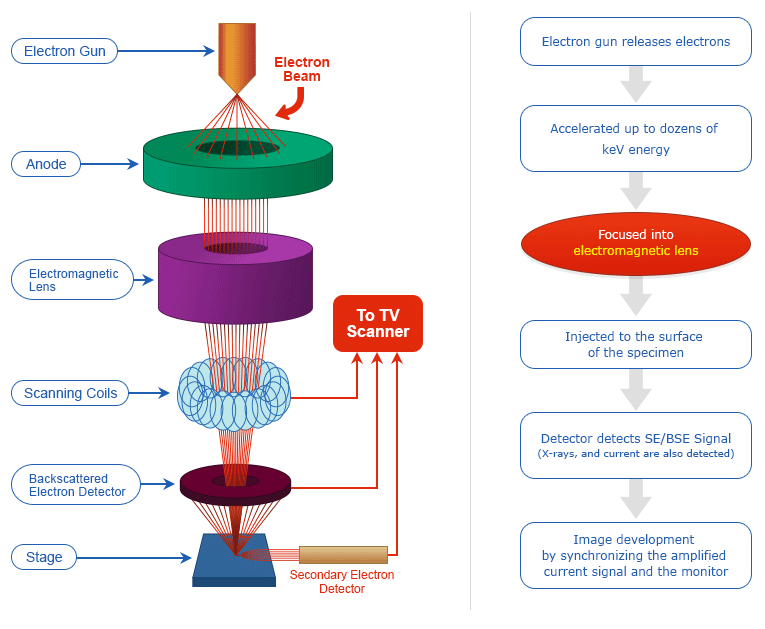
Electron Beam Manipulation
-
How small the size of electron beam shot into specimen can get is the key of high resolution of SEM
-
ELECRTON LENS
– Condenser Lens
-
Reduces crossover made up in Electron gun
-
Controls Spot size
– Objective Lens
-
Changes location of Prove crossover depending on optic axis
-
Focuses image
-
Generating electron ray
-
Lens system controlling electron ray
-
Scan Coil deciding magnification by deciding scanning area on the specimen
-
Stigmator eliminating astigmatism
-
Detector collecting Signal gained from specimen
-
CRT showing information gained from Detector
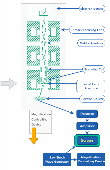
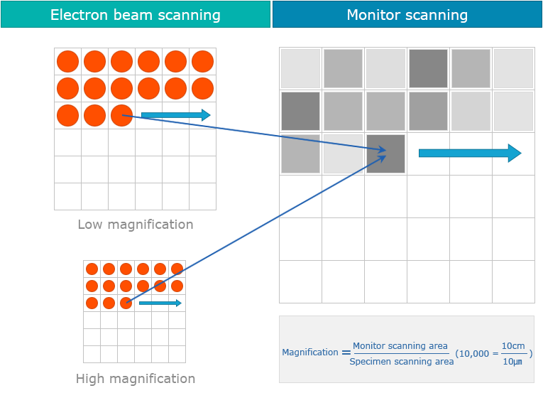
Principle of Magnification of SEM
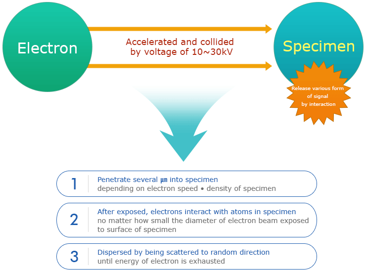
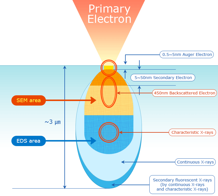
Interaction volume and signal
SE (Secondary Electron) Detector
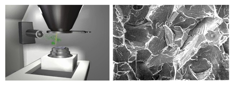
Secondary Electrons generated on the surface of a specimen by the energy gained from inelastic collision with beam electrons. Only a small amount of kinetic energy is transferred to secondary electrons because the amount of energy in beam electron is very small compared to the electrons of specimen.
Most SEMs utilize the Everhart-Thornley (E-T) Detector design. Photons are generated when activated electrons collide with a Scintillator. They then move into a photomultiplier tube by total reflection in an optical waveguide. Photons can go through vacuum and quartz windows because they are in the form of light. Photons attract current from both poles, collect and go back to current at detectable points.
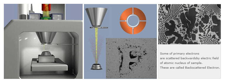
Electrons directed at the sample and are scattered in various directions. These are divided into elastic or inelastic scattering of electron.
Elastic scattering of primary electron – Scattered electrons change momentum but energy changes less that 1eV. Because P=mv and m doesn’t change, only the direction of speed vector changes. Scattering angle is 0-180° and typically 5°. Elastic scattering is generated between negative electron and positive atomic nucleus. Some electrons have large scattering angle to be directed outside the sample and these are backscattered electrons.
Brighter portions of the BSE image above is copper and darker portions are aluminium. Energy during inelastic scattering is transferred to electrons around the atom and kinetic energy in activated electrons is reduced.
Image change depending on Accelerating Voltage
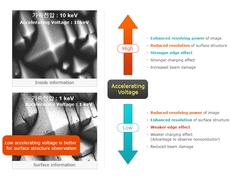
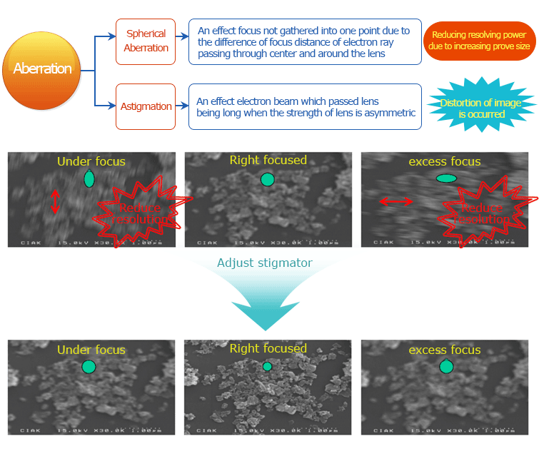
Image distortion depending on Astigmatism
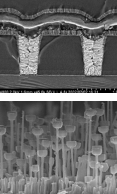
Observation by SEM
Observation of
surface image
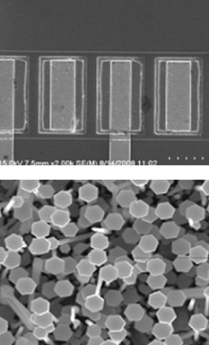
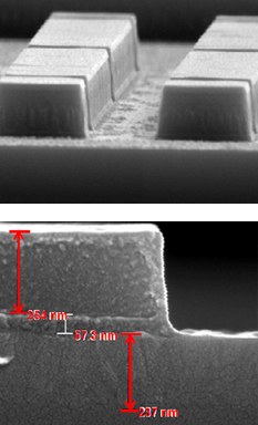
Observation of cross
section structure
Thickness
measurement
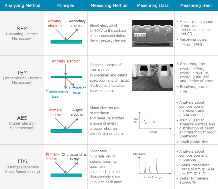
Conclusion. Principle and feature of electron beam analyzing technique
References
-
Principle and Application of electron microscope
-
Analysis of SEM and X-ray microanalysis
SEM Software
The videos below represent some of the capabilities with the software used to operate the SNE-3200 and SNE-4500 SEM systems. Please re-visit this page as we will continue adding new clips about additional features. These videos may not depict the most current capabilities and are intended to provide an example of how the SEM software functions. The most current interface features are listed in the Overview video (bottom).
EDS Elemental Analysis
We will be adding information specific to the Bruker and EDAX EDS Elemental Analysis systems here in the near future. Please Contact Us to request access to some detailed video demonstration of the Bruker ESPIRT software.
In the meantime, please visit the MyScope – EDS Training site for a great overview and background on Energy Dispersive Spectroscopy.
X-Ray Lines for Elements
We have compiled a very useful XLS spreadsheet listing all of the X-Ray peaks or lines using data from several sources such as the Lawrence Berkeley National Laboratory and other nationally recognized resources. The XLS can show either the common lines or all lines. It also highlights the most common overlaps of the major peaks commonly used for micro-analysis. If you would liek a copy of this XLS for your own use, please Contact Us.
Frequently Asked Questions
Here you can find Answers to Frequently Asked Questions and some helpful tips and tricks …
Our Blog

Electron Microscopy: TEM vs. SEM
Electron Microscopy: Transmission Electron Microscopy vs. Scanning Electron Microscopy Electron microscopy is an effective method for obtaining high-resolution images in several fields such as biomedical science, forensics, and technology.

10 Points to Consider when Making Buying Decisions for Tabletop SEM
The market for tabletop Scanning Electron Microscopes has grown significantly due to the global trend toward smaller, faster, and more cost-effective equipment.

